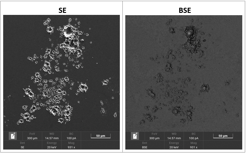
Short Description Allows high quality imaging of poor electrical conductors by both secondary and backscattered electrons Designed for extreme versatility of experimental and characterization approaches. Energy dispersive X-ray analysis allowing identification of elemental distribution from sub-micrometre areas of the specimens.

Description of the technique The Scanning Electron Microscope (SEM) is a TESCAN VEGA 4 equipped with a GMU chamber and a detector for Energy Dispersive X-ray Spectroscopy (EDS). It is also equipped with a Back-Scattered Electron (BSE) detector and it is able to work in low-vacuum (up to 500 Pa) conditions (with nitrogen or water vapour).
Roberto Senesi; Roberto.senesi@uniroma2.it Laboratory: Microscopy
![SEM TESCAN VEGA 3 (SEM_EDS) [0001] with sputtering machine [0041]](https://isis-at-mach.uniroma2.it/wp-content/uploads/2022/12/scheda3.jpg)
TECHNICAL SPECIFICATIONS
- Very wide chamber
- Low vacuum (up to 500 Pa) with nitrogen and water vapour;
AVAILABLE TECHNIQUES
- Scanning Electron Microscopy (SEM)
- Energy Dispersive X-ray Spectroscopy (EDS)
Ancient leather (Museo Egizio); Materials for concentrated solar power;
Cultural Heritage; Energy;
